<tfoot id="j5lkm"><menuitem id="j5lkm"><ul id="j5lkm"></ul></menuitem></tfoot>
    
    
  1. <th id="j5lkm"><progress id="j5lkm"></progress></th>
      <th id="j5lkm"></th>

      <b id="j5lkm"><abbr id="j5lkm"></abbr></b>
      1. <del id="j5lkm"><form id="j5lkm"></form></del>

      2. <strong id="j5lkm"><form id="j5lkm"></form></strong>
          <th id="j5lkm"><progress id="j5lkm"></progress></th>

          Semiconductor Products
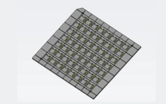
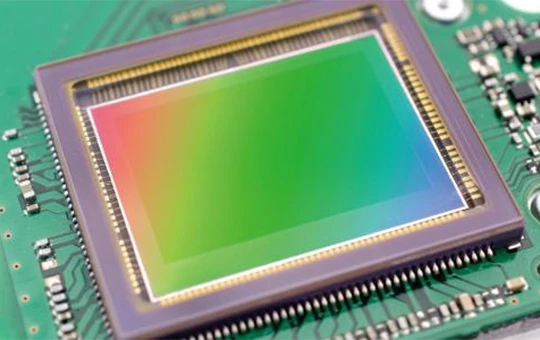
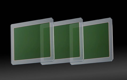
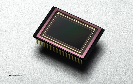
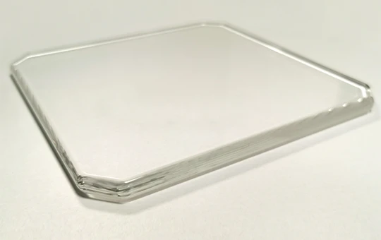
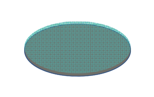
          Ceramic substrate precision machining service
          Application
          Provide precision engineering service on ceramic substrate used for image sensor packages. Printed Circuit Board ceramic substrates are used in image sensor packages for facial recognition, imaging, as well as air pressure sensor packages.
          Optical sensor package substrate
          Application
          Optical sensor packaging substrate, the product has stringent visual requirements (point defects ≤ 6um), mainly used for CCD/CMOS sensor optical packaging of digital cameras.
          Carrier glass substrate (used in support chip)
          Application
          Carrier glass substrate, which requires stringent specification of flatness and roughness used as a component of precision engineering of the biometric chip printed circuit board.
          <tfoot id="j5lkm"><menuitem id="j5lkm"><ul id="j5lkm"></ul></menuitem></tfoot>
            
            
          1. <th id="j5lkm"><progress id="j5lkm"></progress></th>
              <th id="j5lkm"></th>

              <b id="j5lkm"><abbr id="j5lkm"></abbr></b>
              1. <del id="j5lkm"><form id="j5lkm"></form></del>

              2. <strong id="j5lkm"><form id="j5lkm"></form></strong>
                  <th id="j5lkm"><progress id="j5lkm"></progress></th>

                  久久黄网站 | 亚洲无码在线直播 | 99曰高清热视频 | 香蕉视频伊人 | 99黄色视屏 |